Efinix SDRAM Adapter for 6502
This post will be similar to the last post on SDRAM here, but there are some differences.
For one, the Intel SDRAM controller uses the avalon bus, which seems a little simpler than the AXI4 bus that the Efinix one uses. I say that, but I never tried to make it work so I could have just been making it harder on myself for no reason.
Instead of using AXI4, I am using what they call the “native” interface, which has very little overhead but I guess the timings are more important (again maybe AXI4 would have been easier, I just wanted less signals to deal with)
Like the last one, there is an adapter in between the 6502 bus and the memory controller that consists of a state machine to convert the slow and drawn out memory accesses of the 6502 to the quick pulses of the SDRAM.
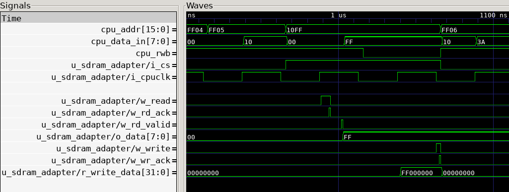
Here is a picture showing this in action. Note in this picture that it is supposed to only be a write, but due to the timing of the absolute memory accesses it appears to do a read and then a write.

Here is an easier to read timing diagram:
Starting with the read, a read is triggered whenever the cpu clock is high, the chip select is high, and rwb is high. The address for the 6502 is valid from negative edge to negative edge, and the data is expected before that second falling edge, so that middle rising edge is the best place to read. We hold the read enable pin high until the controller acknowledges it by raising the rd_ack signal. Once we receive that we stop asserting read enable and wait for the rd_valid signal, which means the data coming out of the controller is valid. In this case, the value is 0xFF. This also happens to be the data that we are writing, since it is what was written to that address the previous time.
Here is an easier to read timing diagram:
The write is very similar, except that the data should be written at the second falling edge, not on the positive edge. Again this absoulte write is a bad example, but just focus during the time when rwb is low and consider that one cycle. normally, data_in would be valid at that rising edge, but often it will be a little bit after which means we can’t latch the data at that edge, and we need to wait until the end of the cycle for it to be valid. When the negative edge occurs, we register the address and the data to write, since the write could overlap the next cycle by a little bit.
Just like the write we raise the write enable signal and wait for the wr_ack signal from the controller. Once we receive that signal we are done though. Note that the “last” signal is rasied at the same time as the read or write enable pins, since we are not doing bursts.
After each access, the state machine goes into a wait state until the chip select is high and the cpu clock is high. At that point, we are in the next cpu cycle ready for a read or write again.
Here is what a write immediately followed by a read would look like.
In reality, all of the sdram signals are much shorter, and the read data comes
well before the falling edge as seen in the above logic analyzer screenshot.
The documentation for the sdram controller is okay, but to be honest just copying the reference design is much easier in terms of the interface designer settings and port declarations.
I did run into a few problems. This first was the sdr_init_done signal. You
have to wait for it to be high before you try to use the memory controller. At
first I had the memory controller reset on the same line as the cpu resset. The
6502 takes 7 cycles after reset to start, which I thought would be enough, but
is not. Also, the cpu may make garbage memory accesses which could try to
access SDRAM when it is not ready. Now when I press the reset button it waits
for the memory controller to initialize before letting the cpu start.
The second problem I had is a stupid one but it still stumped me for a bit. The output of a pll in interface designer can be used as an internal design signal or can be brought out to a pin. I had made a block for the SDRAM clock, but never actually set it to be the output from the PLL. I kept looking at the signals and seeing that they were the exact same as the ones in the manual, but it was not working. Turns out, the SDRAM chip needs a clock signal to work. I suppose the ‘S’ in ‘SDRAM’ is not there for nothing.
As always, the code can be found on my gitlab.