Rebuilding the Breadboard 6502
While I was working on creating graphics using my FPGA (which I’ll get back to eventually), I was also working on moving my 6502 computer from a breadboard to a more permanent setup.
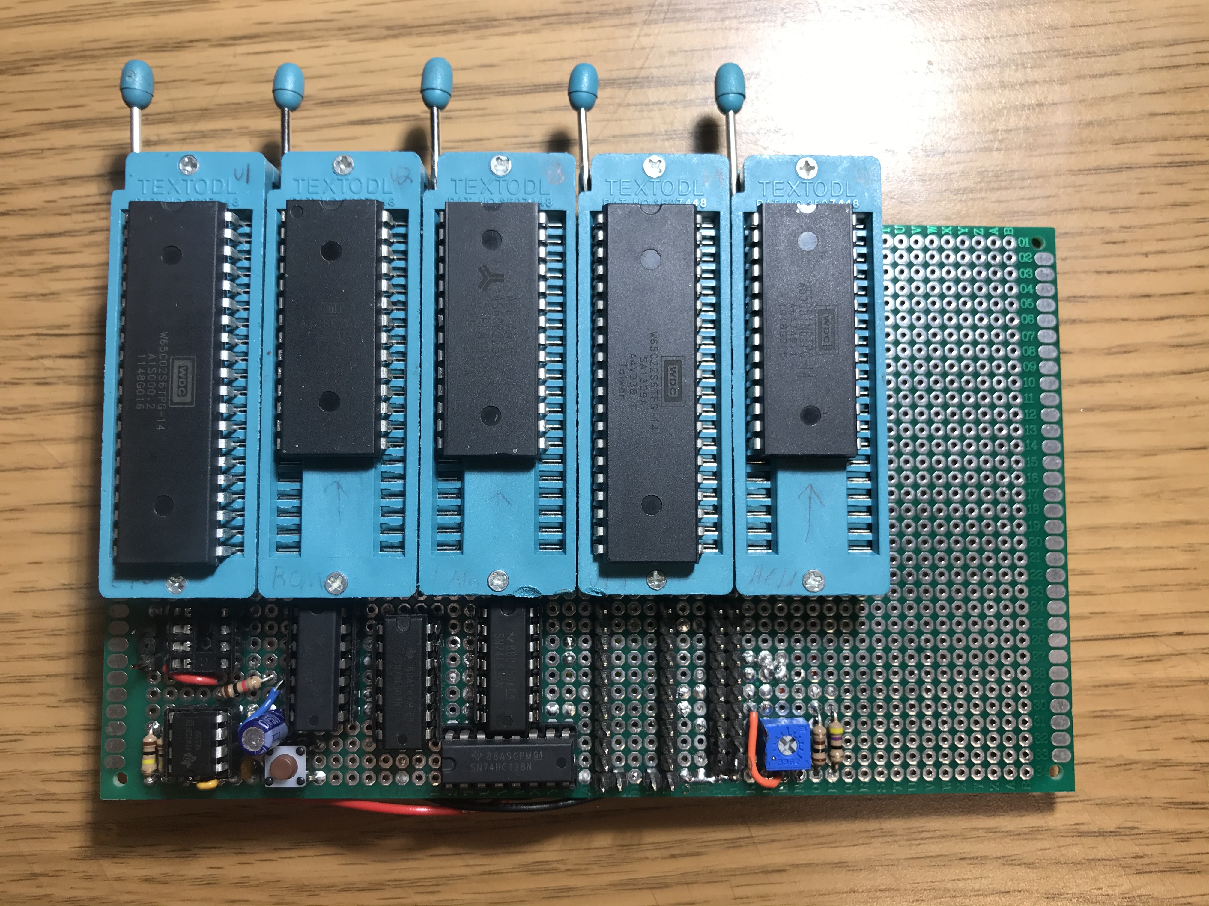
What I came up with was this: 

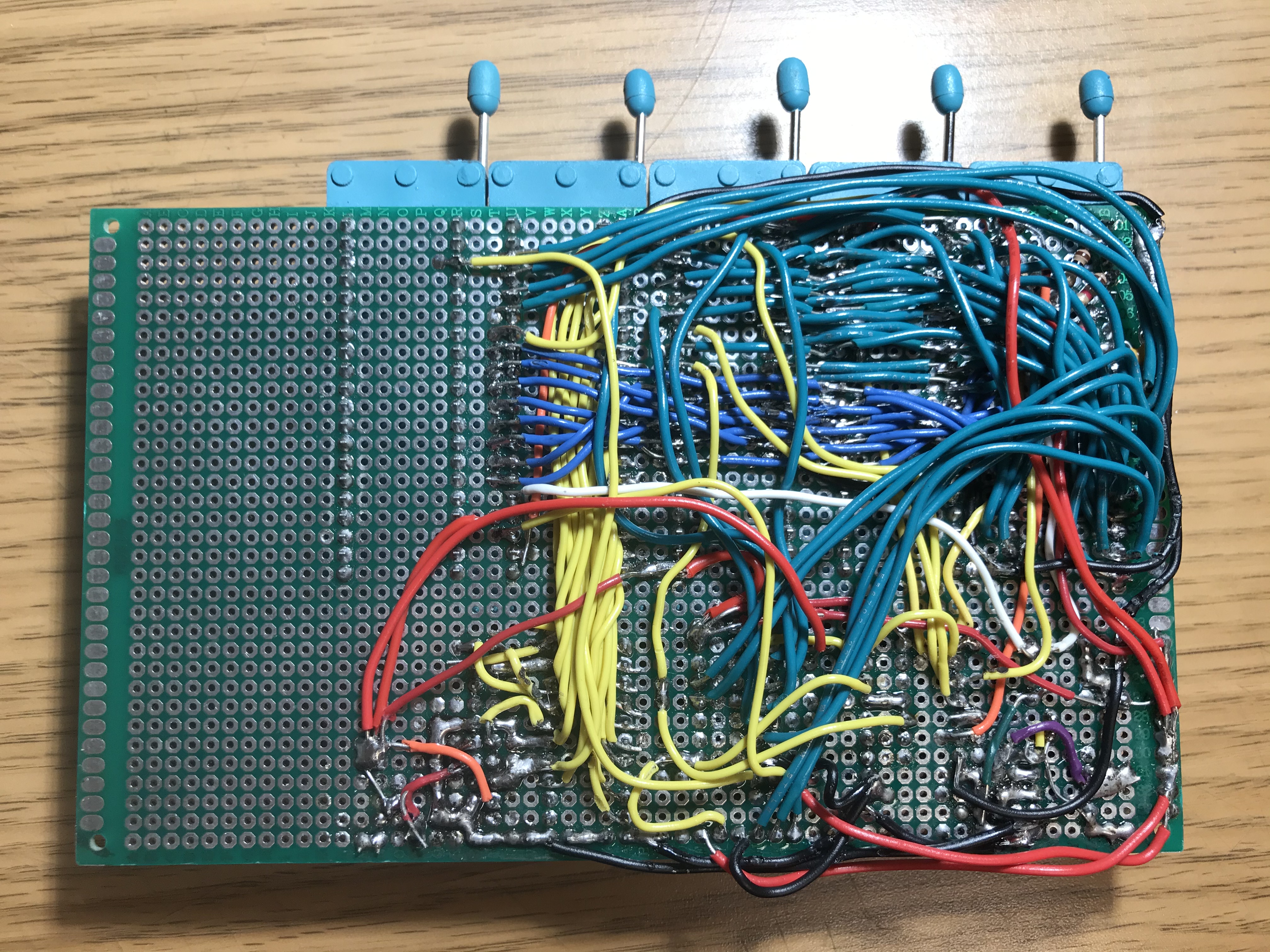
The back looks pretty messy and it’s a pain to work on, but I don’t have proper wire-wrapping stuff and I don’t feel confident enough to make a PCB yet. I’ve worked on it for a bit now but I can’t quite get it to work like it’s supposed too, it keeps resetting randomly.
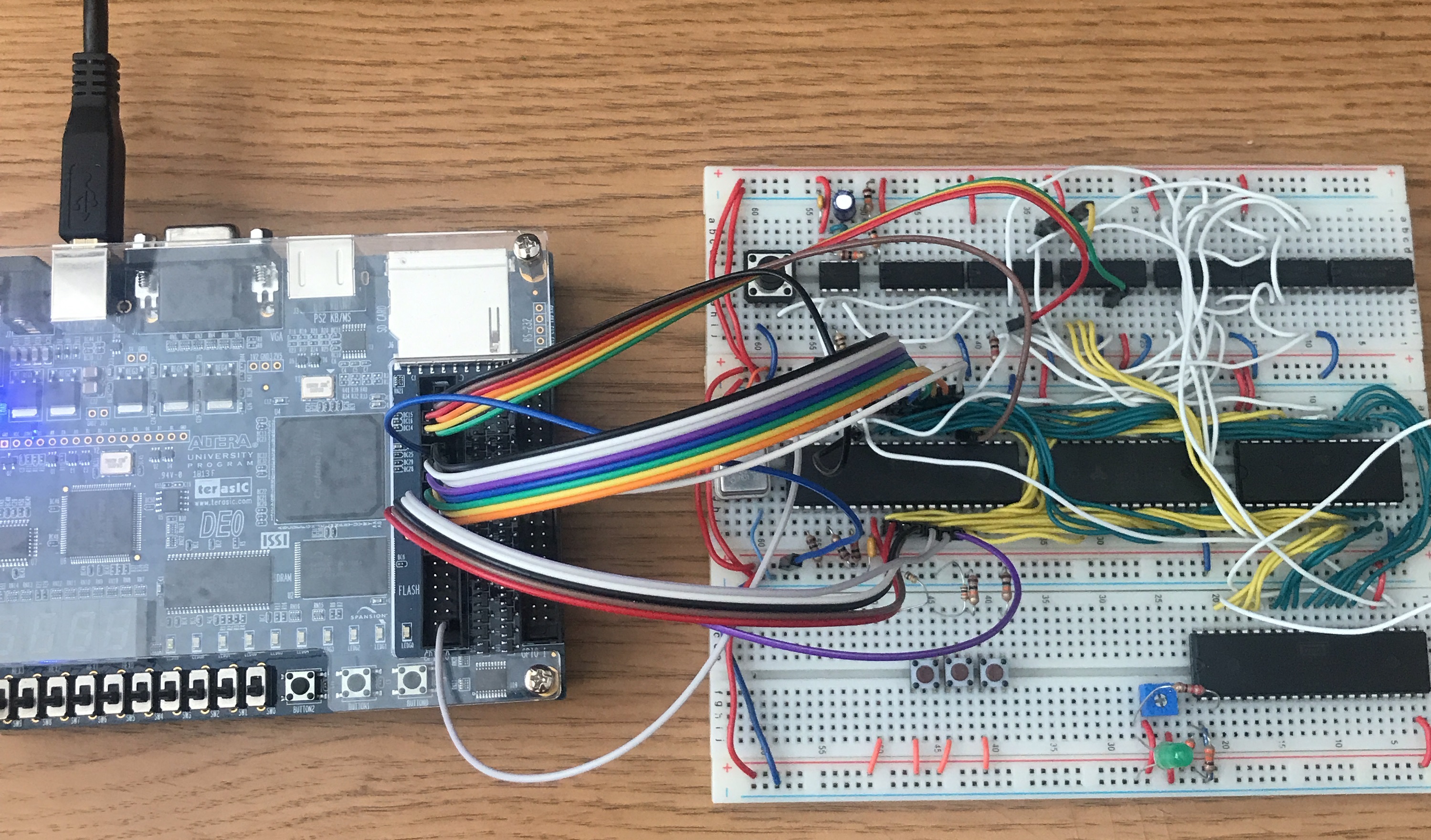
After I burned through another CPU, I bought 3 more as well as a bunch of other necessary components like RAM, ROM, and logic chips. With all these new parts, I had enough to rebuild the original computer on the breadboard where it’s much easier to fix any problems that might arise, so I did.
As usual, I put it together and it didn’t work. I tried debugging it using an LED but it’s too complex to really figure anything out doing that, what I need is a logic analyzer. I’ve mentioned before how I can’t seem to find one at school, but then I remembered something: the FPGA comes with a built in logic analyzer. SignalTap II, part of the Quartus suite, is meant for debugging the inside of the FPGA where you can’t get a physical analyzer, but what I did was make an module in verilog that has 32 inputs and nothing else. When I set up the logic analyzer, I just have it monitor these inputs and I essentially have a 32 channel logic analyzer.
Here’s how that looks: 
And using that, I found that my reset signal was being messed up by the clock wire right next to it. At every pulse of the clock, the reset would pulse for a tiny bit as well, which was enough to mess up the whole circuit. I fixed this by just putting a small capacitor to ground on the reset line which is probably not the ideal way to do this but it seems to work good enough. From there I could start adding more features.
Here is a quick program I wrote to test the RAM:
start:	lda #$00
loop:	sta $00
	lda $00
	adc #$01
	jmp loop
It increases the value of $00 in memory, so the computer must be able to read and write to the RAM for
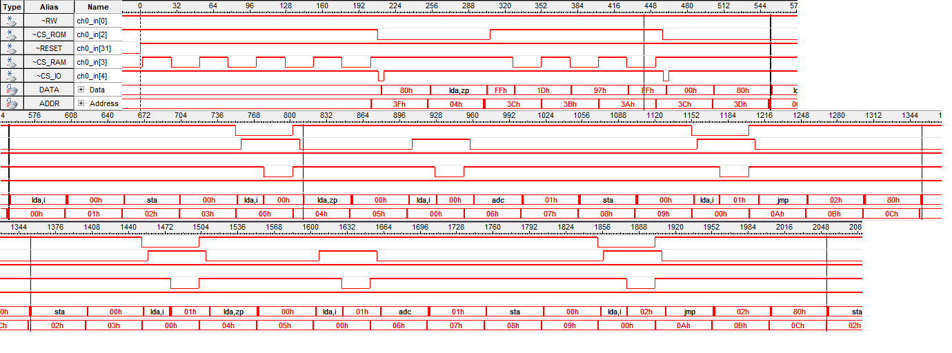
it to work. Here is the resulting waveform: 
Now that is probably really hard to see but I’ll do my best to explain it. The 3rd trace from the top is
the reset line, and a rising edge indicates a reset. After the first rising edge, you can see nothing
really happens at first, and then some random stuff appears. At the end of that random stuff you can
see it loads 00h and 80h on the data line from 3Ch and 3Dh from the address lines. Note that those
should actually be FFFCh and FFFDh but I don’t have all of the address lines hooked up. 00h and 80h
represent the reset vector. The 6502 is little-endian so the vector is $8000. The cpu then starts
running code from $8000. Onto the second row. The first thing it sees at $8000 is the lda #$00 and sta
$00. The little half thing you see with lda,i and 00 is the cpu writing data to RAM. You can see the RW
and CS_RAM lines change to indicate this. The next instruction begins the loop, where it loads the value
from $00, adds 1 to it, then stores it back at $00. You can see following eah sta instruction, the
value being written increases, which means the thing is working.