Adding RAM to the 6502
Picking up where I left off yesterday, the first thing to do was put the RAM chip in. These old 8-bit memory chips (62C256 RAM and 28C256 ROM) are nice in that the pinout is exactly the same, so you don’t need to worry that much when connecting them together. The difference between the two is that for the ROM, the write enable pin isn’t used, but on the RAM it changes with the CPU. Another difference is the output enable pins. Because the ROM can’t be written, OE is connected directly to CE since the only time the chip is used is to read. For the RAM, WE and OE are opposite so the signal is inverted. A15 is connected directly to CE so it’s located from $0000 to $7FFF. This means that there is no room for any IO, but I’ll change that later.
The first thing I tested was writing to ram. This program writes 47 in hex to location $00 in RAM.
start:	lda #$47
	sta $00
	jmp start
a9 47 85 00 4c 00 80
Here is a better look at how I’m checking everything. These are the first 3 bits of the first byte:
(sorry for the glare, next time I’ll bring a USB drive)
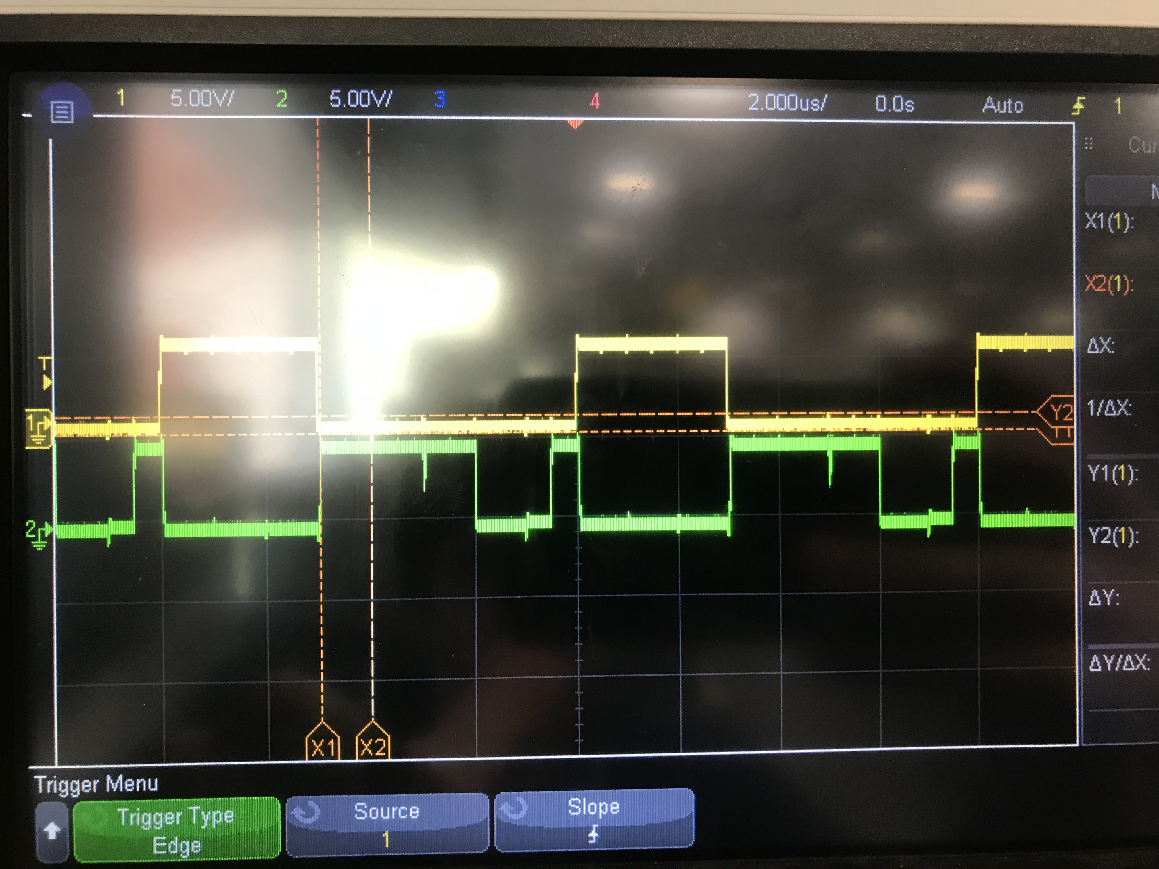
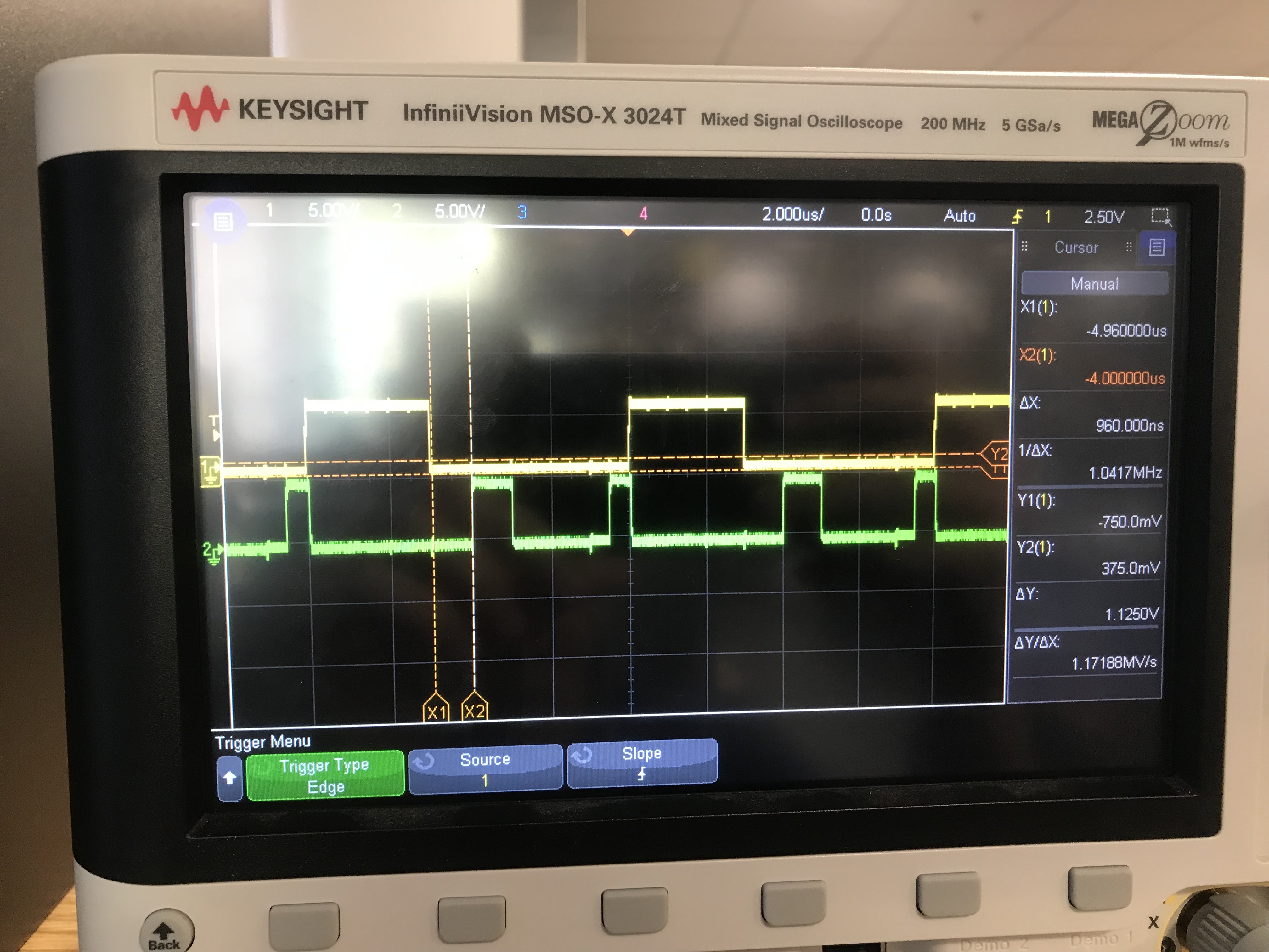
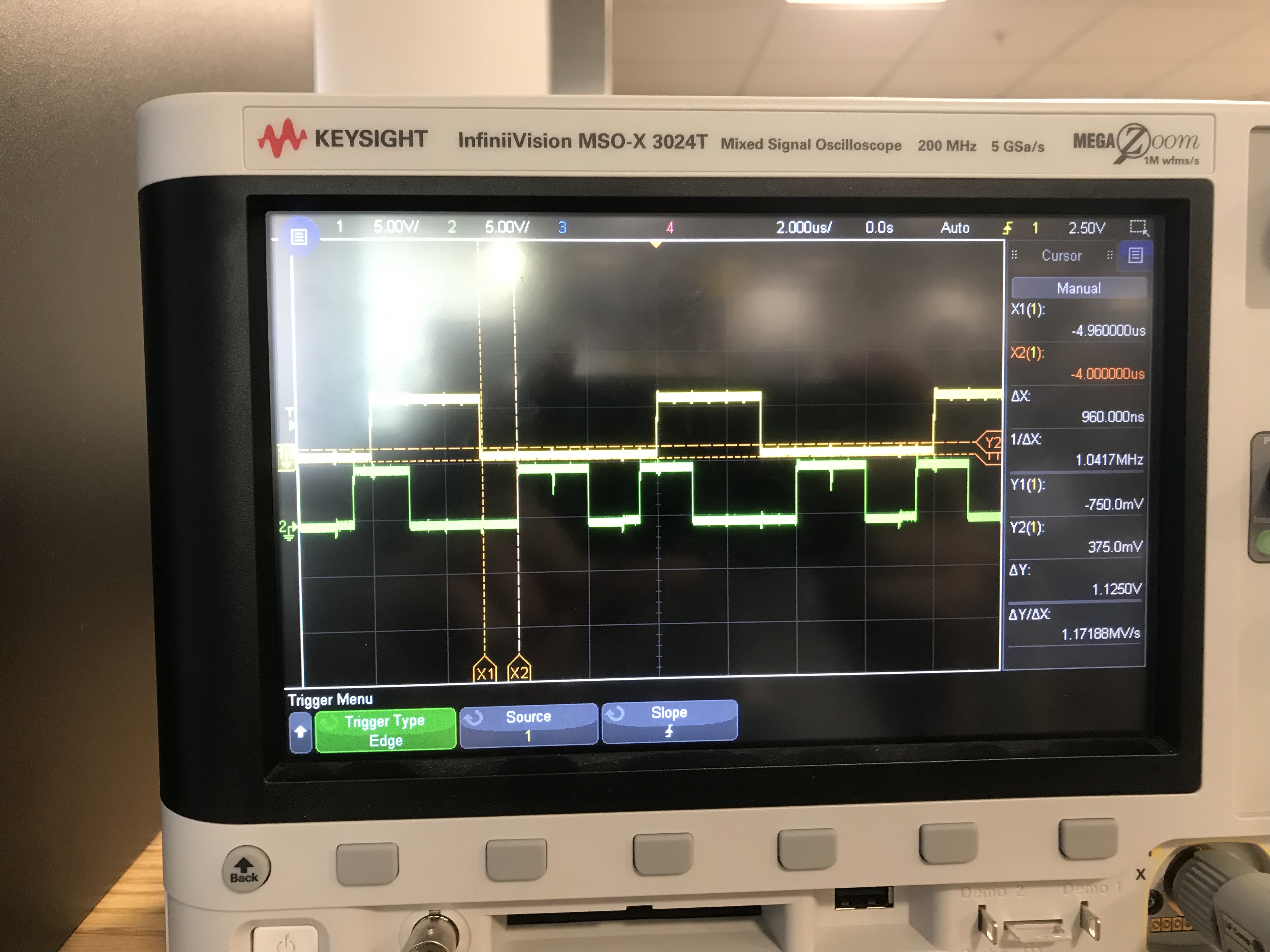
After doing that for all 8 bits of that byte, I move on to the next one.
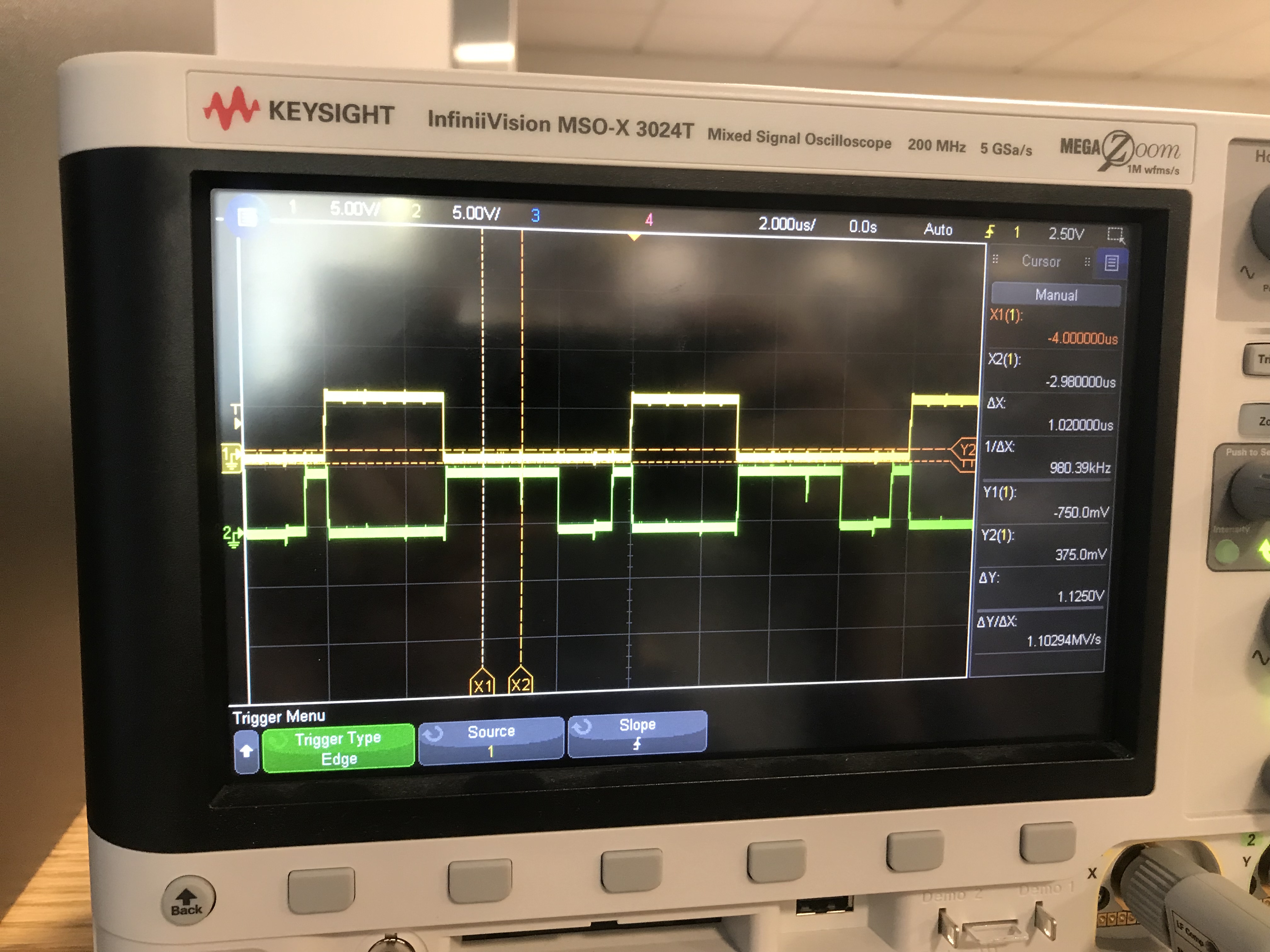
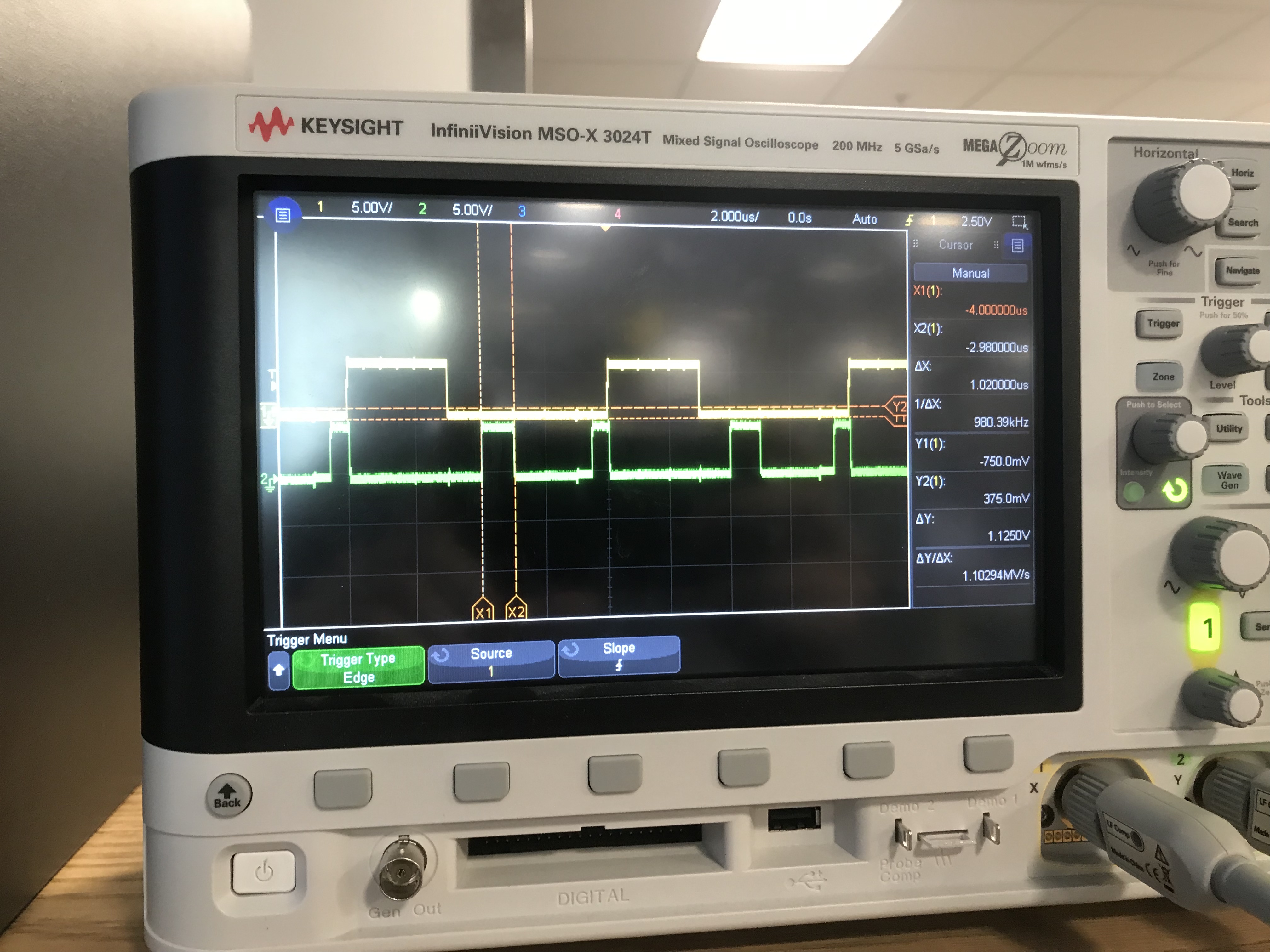
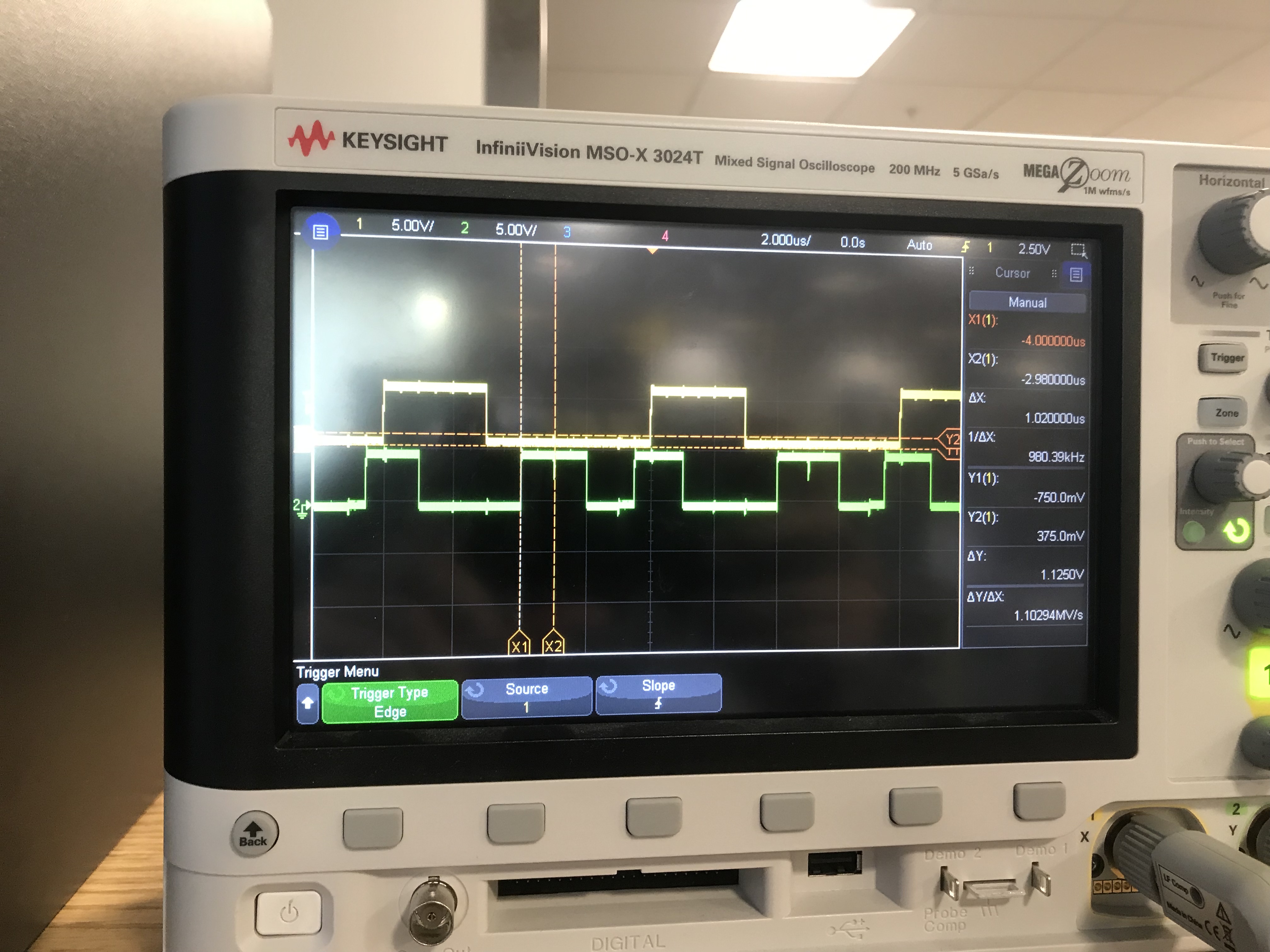
Then I continue on for every byte that I want to check.
The next program starts the same as the first one but it reads from RAM before repeating.
start:	lda #$47
	sta $00
	lda $00
	jmp start
a9 47 85 00 a5 00 4c 00 80
After the a5 00, the correct value showed up on the data bus so I knew the RAM was working.
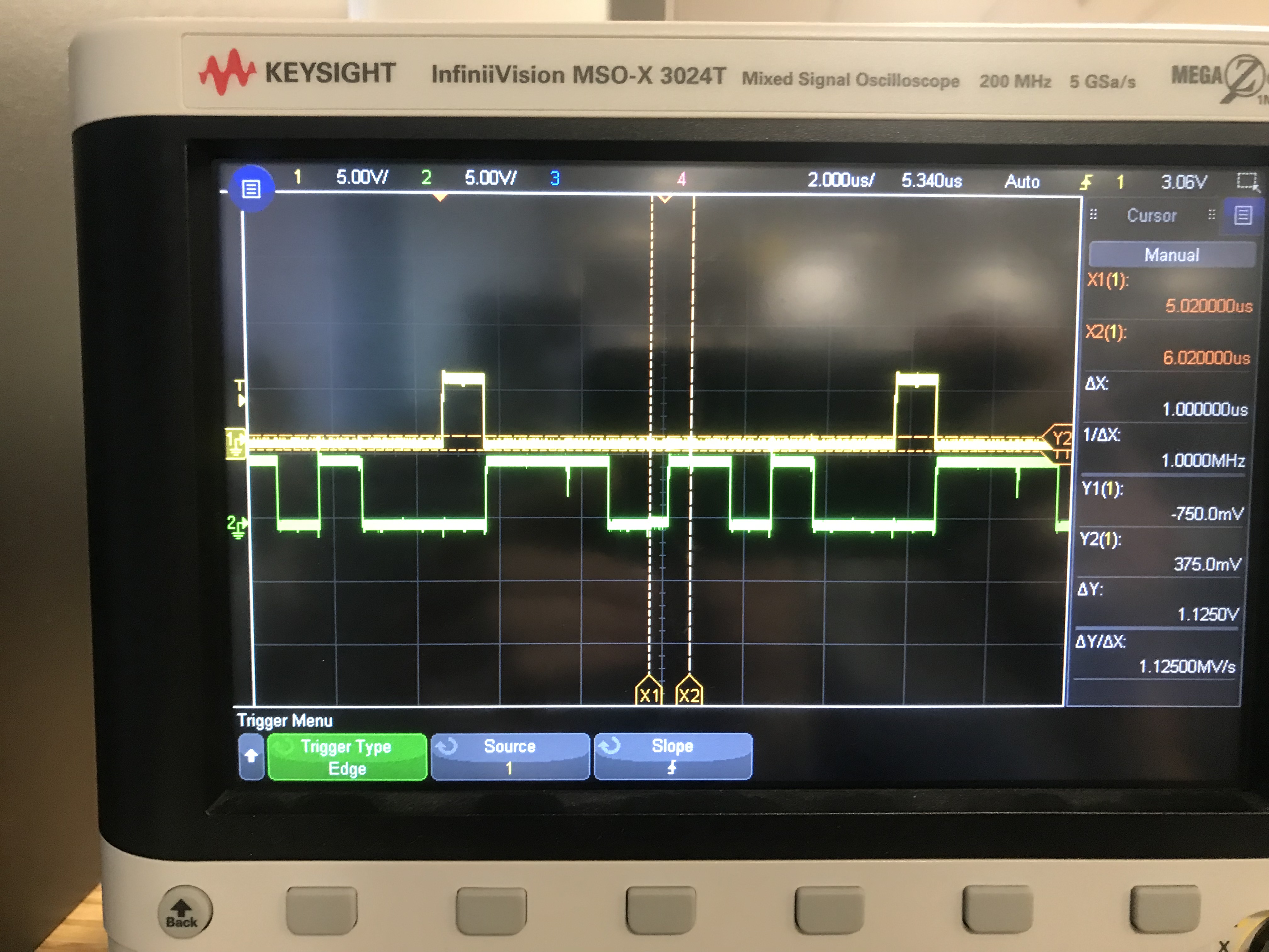
An interesting
thing to note is that when writing to ram, the edge happens during the cycle, not before.
Next time I’ll work on adding IO with a 6522 chip. With that I can light some LEDs or something that gives a better view of the computer actually working.