6502 Computer
I’ve had this 6502 computer project for a few years now but I decided that I am finally going to make it work. Naturally the first step in this process is frying my chip by shorting the power supply across it, but luckily I can just buy a new one.
There are a few resources that I am basing my computer off of, namely Dirk Grappendorf, Ben Eater (who’s 8-bit CPU from scratch I also built), and Grant Searle.

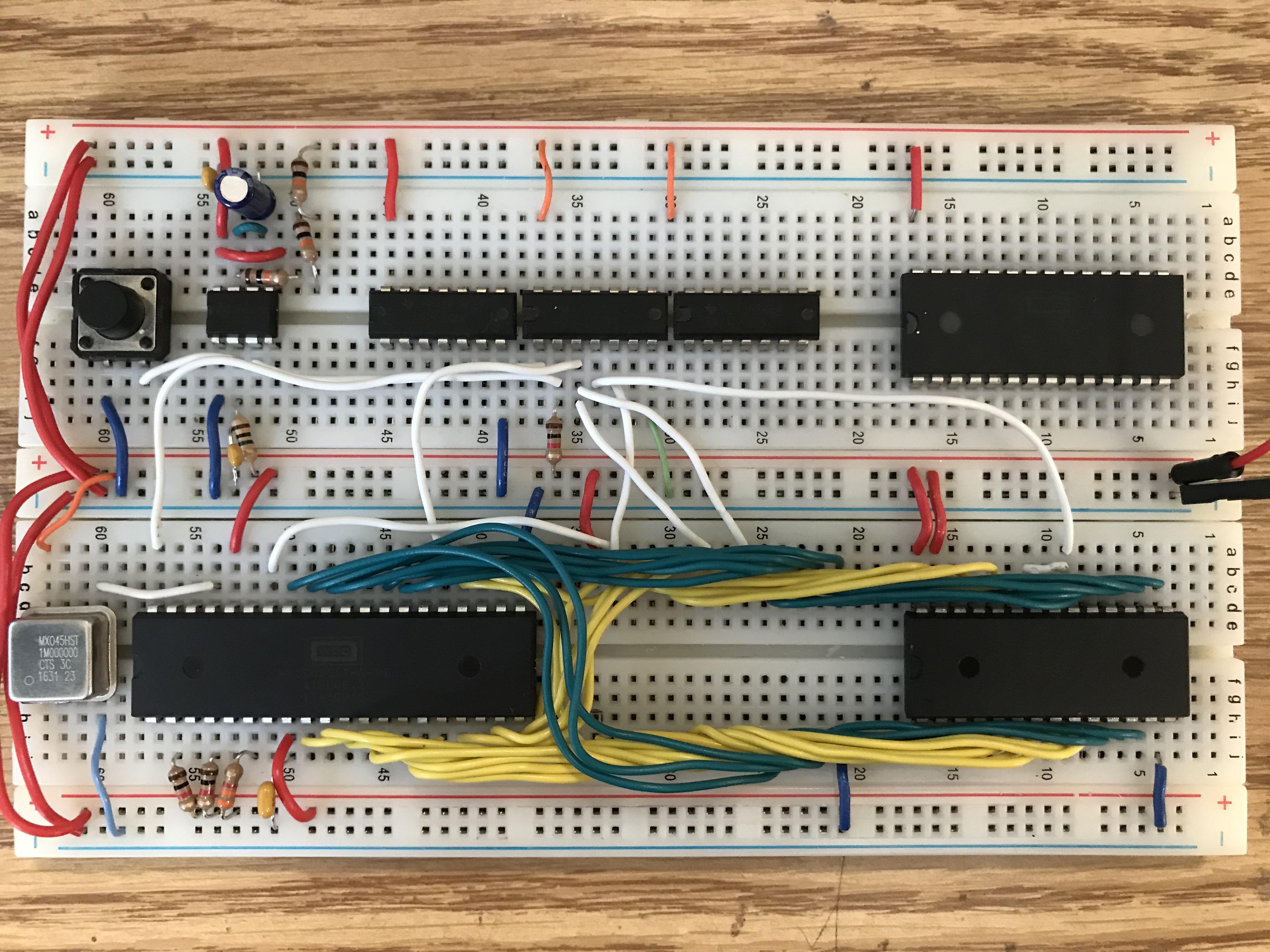
This is what I have come up with so far. Currently it only uses the ROM chip, with the space in the middle ready for the RAM chip when I add it in later.
The ROM chip is an EEPROM, which means you can program and erase it electronically. This is unlike an EPROM, which you have to expose to UV light for while to erase, and is a little more difficult to program. The programmer that I am using is a homebuilt one, based off of Ben Eater’s. His is only made for small programs though, so eventually I’ll need to improve it.


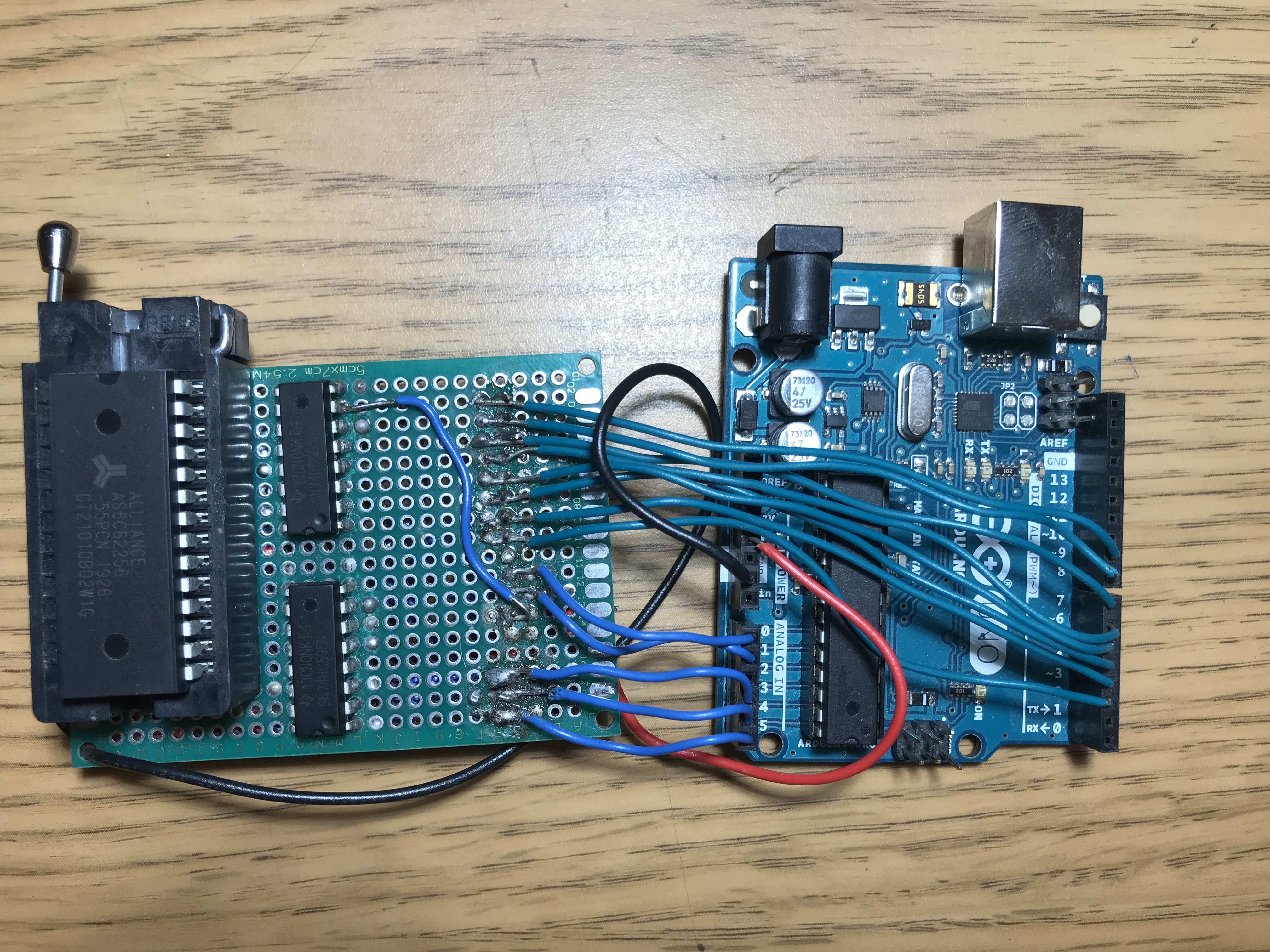
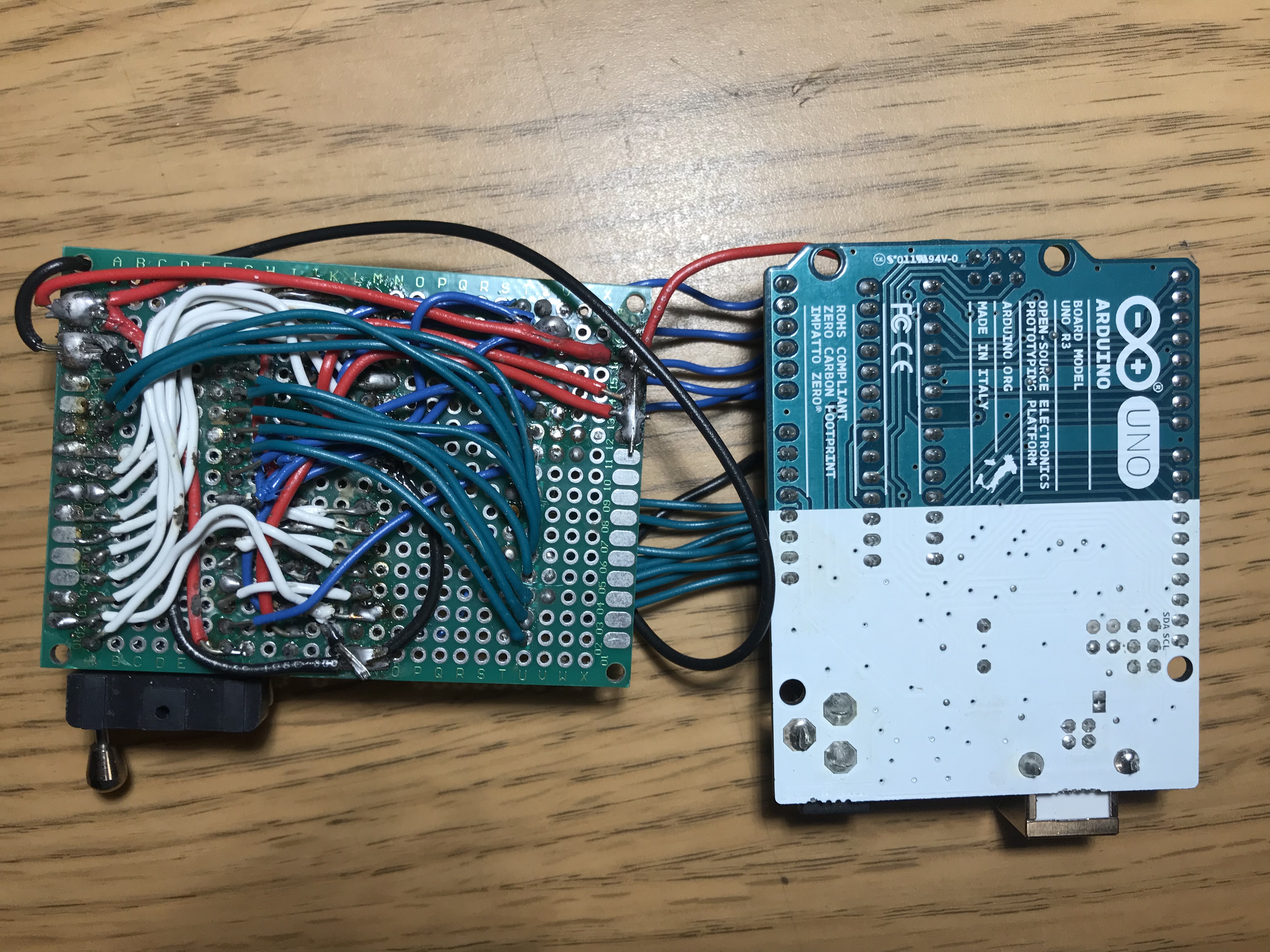
Here’s a quick look at it. You can see it’s made from an Arduino, 2 shift registers, and a ZIF socket. It’s a mess underneath but it works somehow, just don’t ask me to trace it out again. You can tell by the dust on the Arduino that it hasn’t been used for a while
As I said, the firmware is for short programs, which is all I have right now. The first program is a simple infinite loop:
start: jmp startwhich is only 3 bytes: 4c 00 80 (This jumps to memory location $8000, which is $0000 on the ROM chip. I’ll explain this later)
The next program is the same loop but with an extra nop in front, just to make sure it is actually reading the code correctly
start:  nop
        jmp start
This one is just 1 byte longer: ea 4c 00 80
Next I tried a longer one. The instructions at the beginning are irrelevant, they just give more things to test.
start:	inx
	iny
	lda #$47
	jmp start
e8 c8 a9 47 4c 00 80
Now for some reason I can’t seem to find a logic analyzer here at Illinois. I’m sure there’s one around here somewhere, and all of the oscilloscopes have a 16 channel
one built in but they don’t have the cables for them. To test this then, I only had 2 channels of an oscilloscope. The first thing that I did was look at the address
bus to make sure that it was behaving properly. For these short programs, it shouldn’t ever be going past 7 (32775 technically). Once that was good, I could try to
find a pattern that let me know where address 0 was. For some reason, one of the pulses in the sequence was longer than all of the other ones, so if I triggered off
of that one, I could use it it line everything up. With the first probe measuring the A0 pin, which alternates every time the address increases, I used the other probe
to measure each data pin individually. At each address, I looked at the value of the data pin and wrote that down in a table. After doing this for all 8 data pins, I
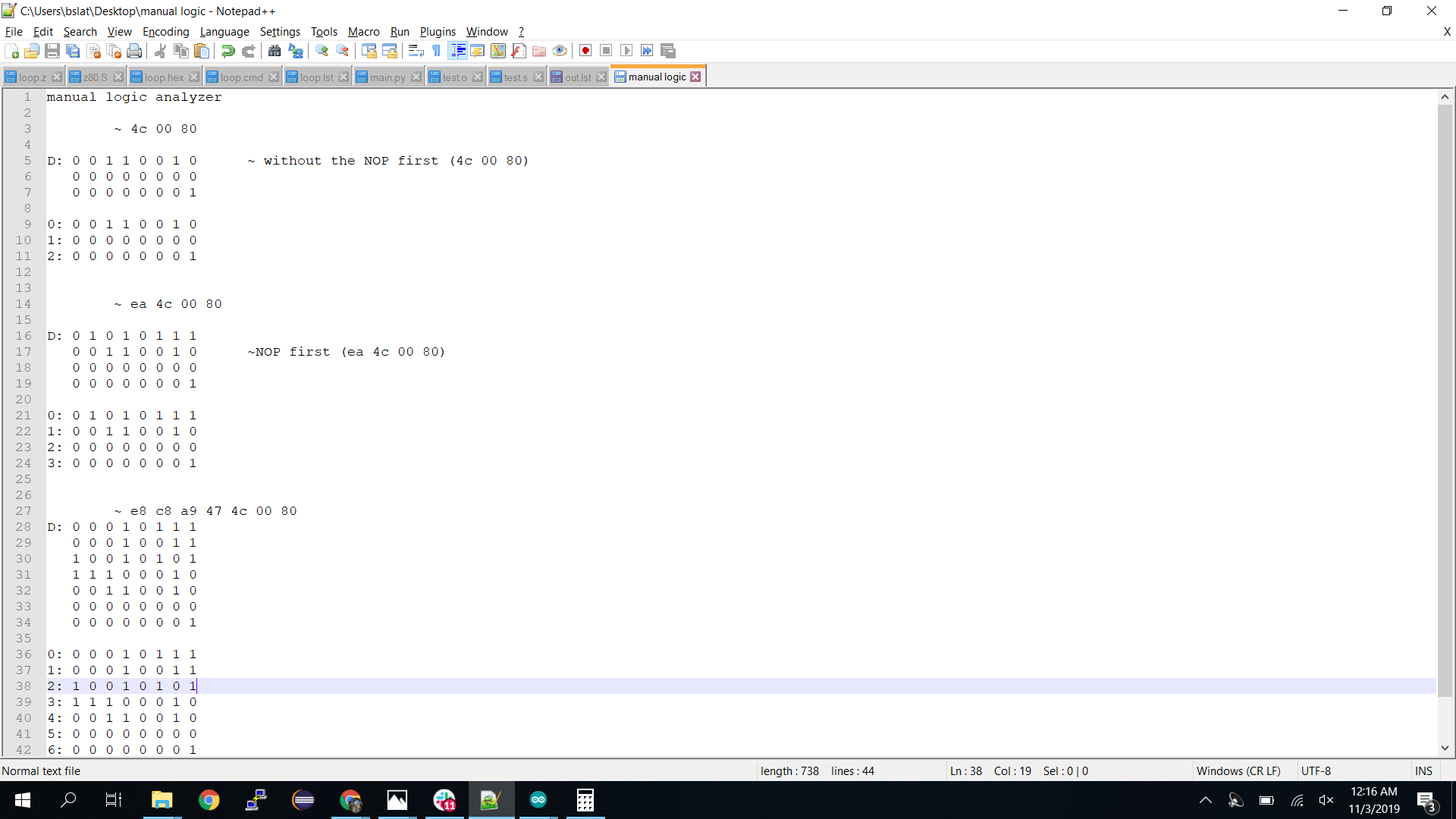
compared what I measured to what the program should be. Here’s a quick shot of what that looked like. After doing this for all 3
programs, everything checked out and I ended up with this table:  .
.
I mentioned before how the beginning of the program was actually at memory location $8000, not at $0000. The 6502 has 16 address lines, meaning it can read 64k of memory, $0000 to $FFFF. The ROM and RAM are each 32k, so one goes on top and one goes on the bottom. When the processor first turns on or is reset, it read from memory location $FFFC and $FFFD to see what to do next. Because those are in the top half, the EEPROM has to go on top. When I am programming the EEPROM, it is programmed starting at it’s own $0000, but because it is wired as the top half of memory, the CPU thinks that it wants to read from $8000. This is what I never understood when I was working on this a cew few years ago, I thought that when you turned on the CPU, it just started reading from address 0. Now though, I know to put $00 at $FFFC and $80 at $FFFD in order for the CPU to start reading where I want it to, and that’s all it took! I’m excited to add more stuff to this computer like RAM, IO, a screen, and eventually I might even write an OS for it.