SD Card for 6502
The one thing that has always stopped me when making these 6502 systems is figuring out how to read data from storage. The first time, I tried using an original Apple IWM with a floppy drive emulator but could not get that to work. The second time, last year, I tried using a USB microcontroller from FTDI, but also could not get that to work. Even earlier with this project I looked to see how much work it would be to use the MAX3421E to read from a USB drive, but didn’t go through with it.
I have finally made some progress using an SD card though. The I/O breakout board that they give us for ECE 385 has a micro SD card slot that can be accessed through SPI.
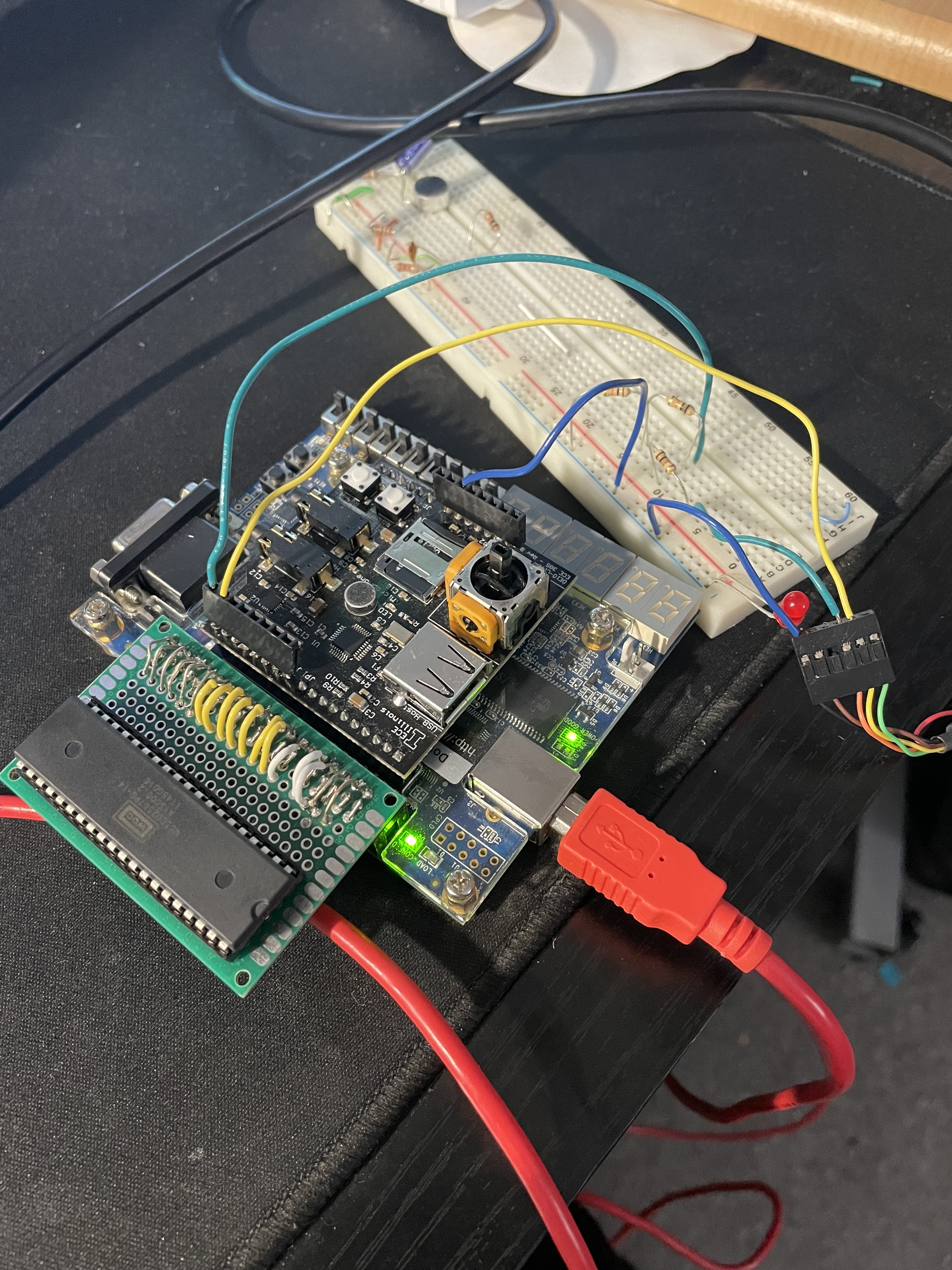
The Shield uses every single pin on the arduino expansion header though, so I had to make a few modifications so that I could keep using the UART. The UART uses the traditional pins 0 and 1, which are sed for an LED and for I2S audio data. The I2S did not end up being a problem, but the LED pin did mess things up. I fixed this by removing the current limiting resistor on one end, so that I could put it back later. I also soldered headers on top of the board so that I could plug the wires back in. Here is a picture of the current setup. The resistors on the breadboard are to convert the data from the computer to 3.3v, since the cable I am using is a 5v one.

As I mentioned, the SD card slot is intended to be used with the SPI protocol, but I decided to use the 1 bit SD protocol instead, since it uses the same pins. It would have been nice to use the 4 bit protocol, it would have been nearly 4 times as fast, but there simply aren’t enough pins available.
The SD protocol uses bidirectional lines for both commands and data, which are handled by using pull up resistors and only driving the lines low. This can be configured inside the FPGA so no external resistors are neccesary (If you are looking in pin planner you need to enable that column).
Commands in the SD protocol are formed as 48 bit words. the first bit is a start bit, and is always 0. The second bit is the transmitter bit, which is always 1. The next six bits are the command number. Following the command are 32 bits for the argument, and finally a CRC7 checksum and a 1 to end the transaction.
The CRC7 is kinda weird, but is pretty easy to calculate with an FPGA, so I made a module that does just that. It does not use any fancy parallel computation, so it takes 40 steps to calculate. Luckily it comes after 40 bits are transmitted so it doesn’t matter.
The interface to the cpu consists of 4 bytes for the command argument, and 1 byte for the command number. Writing the command number also triggers the controller to send that command with the current argument.
What commands do we send though?
Well, the first command that we send is CMD0, which resets every card to the idle state. Next is CMD8, where we tell the card the interface conditions. In our case we tell it the voltage range. This will return a response code, also on the cmd line, that tells us what the card supports. We hope that it supports the same things. We also give it a bit pattern that it will return, so we can confirm that it is reading our commands correctly.
From there we send it ACMD41. To send ACMD commands we first send CMD55, then the command we want, so in this case we send CMD55, then CMD41. CMD41 tells us things like if the card is an SDHC card and what voltages it supports (again?). This command also tells us if the card is busy or ready.
We can also send CMD2, which will tell us some information about the card. I’m using a cheap no name card though, so the name of the product is “SD “, and the serial and revision numbers are all 0.
If we want to talk to the card, we use CMD3, which tells the card to send its RCA, which we can use to identify the card. Following this we do CMD7 and send the RCA to select the card.
With the card selected, we then read data by sending CMD17 with the address of the data we want to read. With SDHC cards, each read always read 512 bytes, and the address is the address of this block. That is how they read more than 4Gb with only a 32 bit address.
One important thing to note about the protocol (Thanks matthew!) is that the data on the lines needs to be latched on the falling edges, so that it will be valid on rising edges. This is done by halving the sd card clock compared to the internal clock.
The SD card controller is kind of a mess if I am being honest. It is based around a state machine and a bunch of counters, you can check it out if you want on my gitlab
So what next? Well there are some issues that I am having reading multiple blocks that I need to solve, but following that I can work on getting file system support and eventually loading and executing programs off of the SD card.