Adding Serial to 6502
The simplest way to get output from the computer is over serial, but since I want to have all peripherals inside the FPGA I decided to write a UART myself.
The first thing I did was add an interrupt system so that the CPU can tell where interrupts came from. All interrupts will go through the FPGA so it can keep track.
Here is what the interrupt system looks like:
always_ff @(posedge clk_50) begin
    if (rst)
        irq_data_out <= '0;
    else if (irq_cs && ~cpu_rwb)
        irq_data_out <= irq_data_out & cpu_data_in;

    else begin
        if (~button_1)
            irq_data_out[0] <= '1;
        if (uart_irq)
            irq_data_out[1] <= '1;
    end

end
button_1 is a button on the board that I was using to test interrupts.
At reset, the interrupt status register is cleared. The cpu can also write to
the cpu status register, but it can only clear bits, not set them. During
normal operation, if one of the interrupt sources is triggered then it sets the
appropriate bit in the irq status register irq_data_out.
The cpu interrupt line is asserted whenever the interrupt status register is not 0:
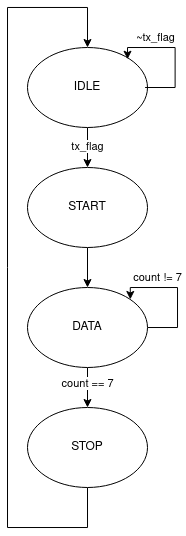
assign cpu_irqb = irq_data_out == 0;Now for the UART. I begin with the transmitter, since it was easier. The logic for the transmitter lies in a finite state machine as follows:

In the IDLE state, the transmitter waits for the cpu to write to the data
transmit buffer. When data is written to that address, it sets tx_flag. At
the next cycle, the transmitter goes into the START state. The START state
simply outputs the start bit, which is 0. It also resets the data bit count
to 0.
The DATA state will output the count bit of the data transmit buffer, then
increments count. In this way it will output the byte LSB first. It is
hardwired to output 8 bits, but this can be changed in the future. Once in the
STOP state, it outputs the stop bit 1 for 1 clock cycle, before returning to
the IDLE state. The STOP state also resets tx_flag to 0, indicating that the
transmitter is ready to transmit another byte.
All of these state transitions are driven by the a clock with the desired baud rate, which in this case is 9600. This is done by dividing the 50MHz clock with a constant. This constant can be changed to select different baud rates, but it is currently hard coded.
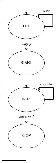
The receiver is similar to the transmitter, in fact it has the same state diagram, but operates in a slightly different way due to the fact that it has to synchronize the clocks when it receives a data packet.

In the IDLE state, the receiver samples RXD to check for a start bit. Supposedly you are supposed to sample at 16x the baud rate, but I just sample it at 50MHz. If this causes problems then I can change it. If a start bit is detected, we go to the START state. The counter for the clock divider is set to half of the constant so that the receive phase is offset from the transmit phase by 90 degrees. This ensures that the data is sampled after it has stabilized. The Start state just goes to the DATA state.
The DATA state works like in the transmitter, where it counts up to 8 before moving to the STOP state. At each cycle in the DATA state, the data in RXD is read into the receive buffer LSB first. The STOP state raises the rx_flag, indicating to the CPU that data is ready to be read. This also raises a UART interrupt. The STOP state then goes back to the IDLE state.
The cpu code is very straightforward:
_uart_txb:
        sta UART_TXB        ; Just write value, don't wait
        rts

_uart_txb_block:
        sta UART_TXB        ; Write value
@1:     lda UART_STATUS     ; Wait for status[0] to be 0
        bit #$01
        bne @1
        rts

_uart_rxb:
        lda UART_RXB        ; Read value
        ldx #$00
        rts

_uart_status:
        lda UART_STATUS
        ldx #$00
        rts
The first function writes the data to the transmit buffer and returns. The second functiion does the same, but then waits for the data to be transmitted before returning. This is the one that I am using.
the receive function reads the data from the receive buffer then returns.
The code can be found on my GitLab
I also host a mirror on GitHub